Polyethylenimine ethoxylated interlayer-mediated ZnO interfacial engineering for high-performance and low-temperature processed flexible perovskite solar cells: A simple and viable route for one-step processed CH3NH3PbI3
- 저자
- Ju Won Lim, Huan Wang, Chi Hun Choi, Li Na Quan, Kyungwha Chung, Won-Tae Park, Yong-Young Noh, Dong Ha Kim*
- 저널명
- Journal of Power Sources, 438, 226956 (2019)
- 년도
- 2019
- Link
- https://doi.org/10.1016/j.jpowsour.2019.226956 551회 연결
[Abstract]
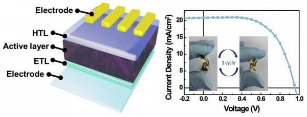
Developing perovskite solar cells (PSCs) with high-efficiency and a low-temperature process has great potential for the realization of the scalable, economic, and roll-to-roll based renewable energy conversion devices. ZnO has been recognized as the promising electron transport layer (ETL) that may overcome the limitations of the conventional TiO2. However, methylammonium lead iodide (MAPbI3) perovskite is prone to decomposition at the ZnO surface, which hinders the development of simple one-step deposition of perovskite, resulting in the limited photovoltaic performance. Herein, we report interlayer mediated efficient ETLs for viable flexible PSCs. The utilization of polyethyleneimine ethoxylated layer on ZnO prevents the direct contact between the perovskite and ETLs, avoiding the photoactive layer decomposition. Thus, interlayer-mediated PSCs show higher efficiency with enhanced stability by decreasing the electron transport barrier. As a result, the PSC employing tailor-designed ETL interfaces exhibited average power conversion efficiency (PCE) of 15.8%, which was superior by 25.4% to that of a control device (12.6%). With our strategy, we further demonstrated PSCs on flexible substrates which exhibit an average PCE of 11.9% under low-temperature fabrication. The new interface engineering strategy may pave the way to the realization of high performance, easy-to-process, and large-area perovskite optoelectronics.
- 이전글Bis-Diketopyrrolopyrrole and Carbazole-Based Terpolymer for High Performance Organic Field-Effect Transistors and Infra-Red Photodiodes 24.12.15
- 다음글Naphthalene flanked diketopyrrolopyrrole: A new DPP family member and its comparative optoelectronic properties with thiophene- and furan-flanked DPP counterparts 24.12.15
