Thickness dependence of a CuI hole transport layer on initial photostability and photovoltaic performance of organic solar cells
- 저자
- Sangcheol Yoon, Hyebin Kim, Eul-Yong Shin, Yong-Young Noh, Byoungchoo Park, Inchan Hwang*
- 저널명
- Physica Status Solidi A, 213, 9, 2431-2437 (2016)
- 년도
- 2016
- Link
- http://dx.doi.org/10.1002/pssa.201600052 648회 연결
[Abstract]
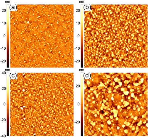
Understanding the effects of interlayers in organic photovoltaic devices is necessary to investigate its potential to maximize efficiencies. Here, we investigate how a solution-processed copper (I) iodide (CuI) hole transport layer (HTL) prepared onto indium tin oxide (ITO) substrates affects the photovoltaic performances of the devices based on Poly(3-hexylthiophene-2,5-diyl) (P3HT):Phenyl-C61-butyric acid methyl ester (PCBM), with its different thicknesses. We found that the film morphology and roughness depends sensitively on the concentration of CuI solutions used for thin films. The surface of CuI films spun with high concentration solutions consists of large grains with high roughness, resulting in a direct short in the devices. For the devices with a thin CuI layer, the power conversion efficiency (PCE) of the devices under illumination was observed to decrease with time. The X-ray photoelectron spectroscopy (XPS) suggests that the indium ions might be diffused into the active layer across the thin CuI layer. Our results highlight that the CuI layer thickness is a key parameter in affecting not only efficiency but also device yield and short-term photostability.
