Large-scale organic nanowire lithography and electronics
- 저자
- Sung-Yong Min, Tae-Sik Kim, Beom Joon Kim, Himchan Cho, Yong-Young Noh, Hoichang Yang, Jeong Ho Cho, and Tae-Woo Lee*
- 저널명
- Nature Communications, 4, 1773 (2013)
- 년도
- 2013
- Link
- http://dx.doi.org/10.1038/ncomms2785 1036회 연결
[Abstract]
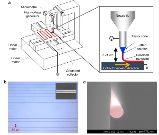
Controlled alignment and patterning of individual semiconducting nanowires at a desired position in a large area is a key requirement for electronic device applications. High-speed, large-area printing of highly aligned individual nanowires that allows control of the exact numbers of wires, and their orientations and dimensions is a significant challenge for practical electronics applications. Here we use a high-speed electrohydrodynamic organic nanowire printer to print large-area organic semiconducting nanowire arrays directly on device substrates in a precisely, individually controlled manner; this method also enables sophisticated large-area nanowire lithography for nano-electronics. We achieve a maximum field-effect mobility up to 9.7 cm2 V−1 s−1 with extremely low contact resistance (<5.53 Ω cm), even in nano-channel transistors based on single-stranded semiconducting nanowires. We also demonstrate complementary inverter circuit arrays comprising well-aligned p-type and n-type organic semiconducting nanowires. Extremely fast nanolithography using printed semiconducting nanowire arrays provide a simple, reliable method of fabricating large-area and flexible nano-electronics.
