Effects of gate dielectrics and their solvent on characteristics of printed n-channel polymer field-effect transistors
- 저자
- Kang-Jun Baeg, Antonio Facchetti, and Yong-Young Noh*
- 저널명
- Journal of Materials Chemistry C, 22, 21138-21143 (2012)
- 년도
- 2012
- Link
- http://dx.doi.org/10.1039/C2JM34218A 573회 연결
[Abstract]
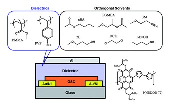
In this study, we investigated the effects of polymer gate dielectrics and their solvents on the characteristics of n-channel top-gate-structured organic field-effect transistors (OFETs) that used poly{[N,N-9-bis(2-octyldodecyl)-naphthalene-1,4,5,8-bis(dicarboximide)-2,6-diyl]-alt-5,59-(2,29-bithiophene)} (P(NDI2OD-T2)) (ActivInk™ N2200). The characteristics of P(NDI2OD-T2)-based OFETs are strongly dependent on the chemical properties of the polymer gate dielectrics used and the morphology of the semiconductor–dielectric interface, which is dependent of the dielectric solvent used for dielectric-layer deposition. Both spin-coated and inkjet-printed P(NDI2OD-T2)-based FETs exhibited reasonably high values of field-effect mobility (μFET) at 0.1–0.3 cm2 V−1 s−1 with poly(methyl methacrylate) as the gate dielectric and a number of carefully selected orthogonal solvents. The value of μFET decreased to 0.03 cm2 V−1 s−1 for a solvent with poor orthogonality (1,2-dichloroethane). This was due to the semiconductor–dielectric interface being rough owing to the dissolution and/or swelling of the underlying P(NDI2OD-T2) layer. In addition, the value of μFET decreased dramatically, to 0.005 cm2 V−1 s−1, with poly(4-vinyl phenol) (PVP) as the dielectric material, dissolved in a perfectly orthogonal solvent (1-butanol). This was due to electron trapping by the hydroxyl groups in PVP.
