Highly stable printed polymer field-effect transistors and inverters via polyselenophene conjugated polymers
- 저자
- Dongyoon Khim, Woo-Hyung Lee, Kang-Jun Baeg, Dong-Yu Kim, In-Nam Kang and Yong-Young Noh*
- 저널명
- Journal of Materials Chemistry C, 22, 12774-12783 (2012)
- 년도
- 2012
- Link
- http://dx.doi.org/10.1039/c2jm16546e 553회 연결
[Abstract]
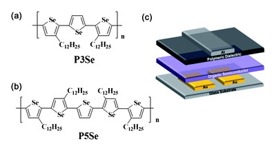
We report the use of two polyselenophene-based conjugated polymers, poly(3,3′′-didodecyl-2,2′:5,2′′-terselenophene) (P3Se) and poly(3,3′′,3′′′,3′′′′-tetradodecyl-2,5′:2′,2′′:5′′,2′′′-pentaselenophene) (P5Se), as an active layer of printed p-channel organic field-effect transistors (OFETs). Top-gate/bottom-contact (TG/BC) P5Se OFETs showed a high-saturation hole mobility of up to ∼0.1 cm2 V−1 s−1 and a high on/off ratio of ∼105 with no hysteresis. In addition, polyselenophene-based OFETs exhibited a much better bias and ambient stability when compared with poly(3-hexylthiophene)-based OFETs. The excellent air stability of those polyselenophenes enables the realization of complementary metal-oxide semiconductor (CMOS) inverters via extended periods of ink-jetting under ambient conditions. CMOS inverters were demonstrated using p-[P5Se] and n-channel [poly{[N,N′-bis(2-octyldodecyl)-naphthalene-1,4,5,8-bis(dicarboximide)-s,6-diyl]-alt-5,5′-(2,2′-dithiophene)}] ([P(NDI2OD-T2)], Polyera ActivInk N2200/OFETs) by inkjet printing of conjugated polymers. Printed CMOS inverters exhibited a stable voltage transfer characteristic with negligible hysteresis, a DC voltage gain of ∼10, and a power consumption of ∼0.025 mW at VDD = −60 V.
- 이전글Gold nanoparticle-doped graphene nanosheets: sub-nanosized gold clusters nucleate and grow at the nitrogen-induced defects on graphene surfacesnucleate and grow at the nitrogen-induced defects on graphene surfaces 24.12.11
- 다음글High-Performance Top-Gated Organic Field-Effect Transistor Memory using Electrets for Monolithic Printed Flexible NAND Flash Memory 24.12.11
