All-Solution-Processed High-Performance MoS2 Thin-Film Transistors with a Quasi-2D Perovskite Oxide Dielectric
- 저자
- Su-Yeon Joung˚, Haena Yim˚, Donghun Lee, Jaehyung Shim, So Yeon Yoo, Yeon Ho Kim, Jin Seok Kim, Hyunjun Kim, Seok-Ki Hyeong, Junhee Kim, Yong-Young Noh*, Sukang Bae*, Myung Jin Park*, Ji-Won Choi*, Chul-Ho Lee*
- 저널명
- ACS Nano, 18, 3, 1958-1968 (2024)
- 년도
- 2024
- Link
- https://doi.org/10.1021/acsnano.3c06972 627회 연결
[Abstract]
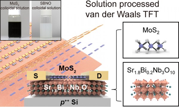
Assembling solution-processed van der Waals (vdW) materials into thin films holds great promise for constructing large-scale, high-performance thin-film electronics, especially at low temperatures. While transition metal dichalcogenide thin films assembled in solution have shown potential as channel materials, fully solution-processed vdW electronics have not been achieved due to the absence of suitable dielectric materials and high-temperature processing. In this work, we report on all-solution-processedvdW thin-film transistors (TFTs) comprising molybdenum disulfides (MoS2) as the channel and Dion–Jacobson-phase perovskite oxides as the high-permittivity dielectric. The constituent layers are prepared as colloidal solutions through electrochemical exfoliation of bulk crystals, followed by sequential assembly into a semiconductor/dielectric heterostructure for TFT construction. Notably, all fabrication processes are carried out at temperatures below 250 °C. The fabricated MoS2 TFTs exhibit excellent device characteristics, including high mobility (>10 cm2 V-1 s-1) and an on/off ratio exceeding 106. Additionally, the use of a high-k dielectric allows for operation at low voltage (∼5 V) and leakage current (∼10–11 A), enabling low power consumption. Our demonstration of the low-temperature fabrication of high-performance TFTs presents a cost-effective and scalable approach for heterointegrated thin-film electronics.
