Improving solution-processed n-type organic field-effect transistors by transfer-printed metal/semiconductor and semiconductor/semiconductor heterojunctions
- 저자
- Chuan Liu, Yong Xu, Zhihong Liu, Hoi Nok Tsao, Klus Mullen, Takeo Minari, Yong-Young Noh*, Henning Sirringhaus
- 저널명
- Organic Electronics, 15, 4, 1884-1889 (2014)
- 년도
- 2014
- Link
- http://dx.doi.org/10.1016/j.orgel.2014.04.032 357회 연결
[Abstract]
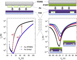
Solution-processed n-type organic field effect transistors (OFETs) are in need of proper metal contact for improving injection and mobility, as well as balanced hole mobility for building logic circuit units. We address the two distinct problems by a simple technique of transfer-printing. Transfer-printed Au contacts on a terrylene-based semiconductor (TDI) significantly reduced the inverse subthreshold slope by 5.6 V/dec and enhanced the linear mobility by over 5 times compared to evaporated Au contacts. Hence, devices with a high-work-function metal (Au) are comparable with those with low-work-function metals (Al and Ca), indicating a fundamental advantage of transfer-printed electrodes in electron injection. We also transfer-printed a poly(3-hexylthiophene) (P3HT) layer onto TDI to construct a double-channel ambipolar transistor by a solution process for the first time. The transistor exhibits balanced hole and electron mobility (3.0 × 10⁻³ and 2.8 × 10⁻³ cm2 V−1 s−1) even in a coplanar structure with symmetric Au electrodes. The technique is especially useful for reaching intrinsic mobility of new materials, and enables significant enlargement of the material tanks for solution-processed functional heterojunction OFETs.
- 이전글Side chains contributions to characteristics of resistive memory based on water-soluble polyfluorenes: Effects of structure and length of side pendant group 24.12.15
- 다음글Simultaneous Enhancement of Electron Injection and Air Stability in N-Type Organic Field-Effect Transistors by Water-Soluble Polyfluorene Interlayers 24.12.15
