A Self-aligned High Resolution Patterning Process for Large Area Printed Electronics
- 저자
- Won Tae Park*, Yong-Young Noh*
- 저널명
- Journal of Materials Chemistry C, 5, 6467-6470 (2017)
- 년도
- 2017
- Link
- https://doi.org/10.1039/C7TC01590A 483회 연결
[Abstract]
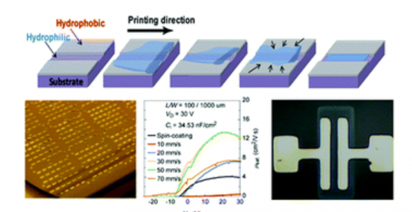
In the production of printed electronic devices, a reliable, high resolution, and cost-effective patterning method is highly required. Here, we report a facile self-aligned patterning process compatible with directional coating processes for manufacturing printed electronic devices. For the self-aligned and high resolution patterning, a hydrophobic self-assembled monolayer (SAM) is formed on a substrate surface and defined at a specific area by irradiation of 172 nm UV light (9–10 mW cm−2) for 3 min through a photomask. A functional hydrophilic ink is coated on the pre-patterned SAM surface by a wire bar-coating process. Using this process, the ink is automatically patterned down to theoretically 2 μm resolution on the bare surface without a hydrophobic SAM by completely dewetting the ink from the SAM surface. We demonstrate high performance metal oxide thin-film transistors (TFTs) with a patterned sol–gel processed indium gallium zinc oxide (IGZO) film by a single bar coating process. The IGZO TFTs show a reasonably high electron mobility of 12.78 cm2 V−1 s−1 with silicon dioxide gate dielectrics and a standard deviation of 21.84% in a 4-inch substrate scale device array.
- 이전글Anodically grown binder-free nickel hexacyanoferrate film: towards efficient water reduction and hexacyanoferrate film based full device for overall water splitting 24.12.15
- 다음글Effect of pre-aggregation in conjugated polymer solution on performance of diketopyrrolopyrrole-based organic field-effect transistors 24.12.15
