Improved ambipolar charge injection in organic field-effect transistors with low cost metal electrode using polymer sorted semiconducting carbon nanotubes
- 저자
- Seung-Hoon Lee, Dong-Yu Kim, Yong-Young Noh
- 저널명
- Organic Electronics, 46, 28-34 (2017)
- 년도
- 2017
- Link
- https://doi.org/10.1016/j.orgel.2017.04.004 442회 연결
[Abstract]
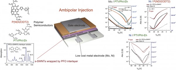
Solution-processed thin film transistors can be implemented using simple and low cost fabrication, and are the best candidates for commercialization due to their application to a range of wearable electronics. We report an ambipolar charge injection interlayer that can improve both hole and electron injection in organic field-effect transistors (OFETs) with inexpensive source-drain electrodes. The solution processed ambipolar injection layer is fabricated by selective dispersion of semiconducting single walled carbon nanotubes using poly(9,9-dioctylfluorene). OFETs with molybdenum (Mo) contacts and interlayer (Mo/interlayer OFETs) exhibit superior performance, including higher hole and electron mobilities, device yield, lower threshold voltages, and lower trap densities than those of bare transistors. While OFETs with Mo contacts show unipolar p-type behaviour, Mo/interlayer OFETs display ambipolar transport due to significant enhancement of electron injection. In the p-type region, transistor performance is comparable to devices with gold (Au). Hole mobility is increased approximately ten-fold over devices with only Mo contacts. The electron mobility of Mo/interlayer OFETs is 0.05 cm2V−1s−1, which is higher than devices with Au electrodes. The p-type contact resistances of Mo/interlayer OFETs are half those of OFETs with Mo contacts. Trap density in Mo/interlayer OFETs is one order magnitude lower than that of pristine devices. We also demonstrate that this approach is extendible to other metals (nickel) and n-type semiconductors with different energy levels. Injection by tunnelling is suggested as the mechanism of ambipolar injection.
